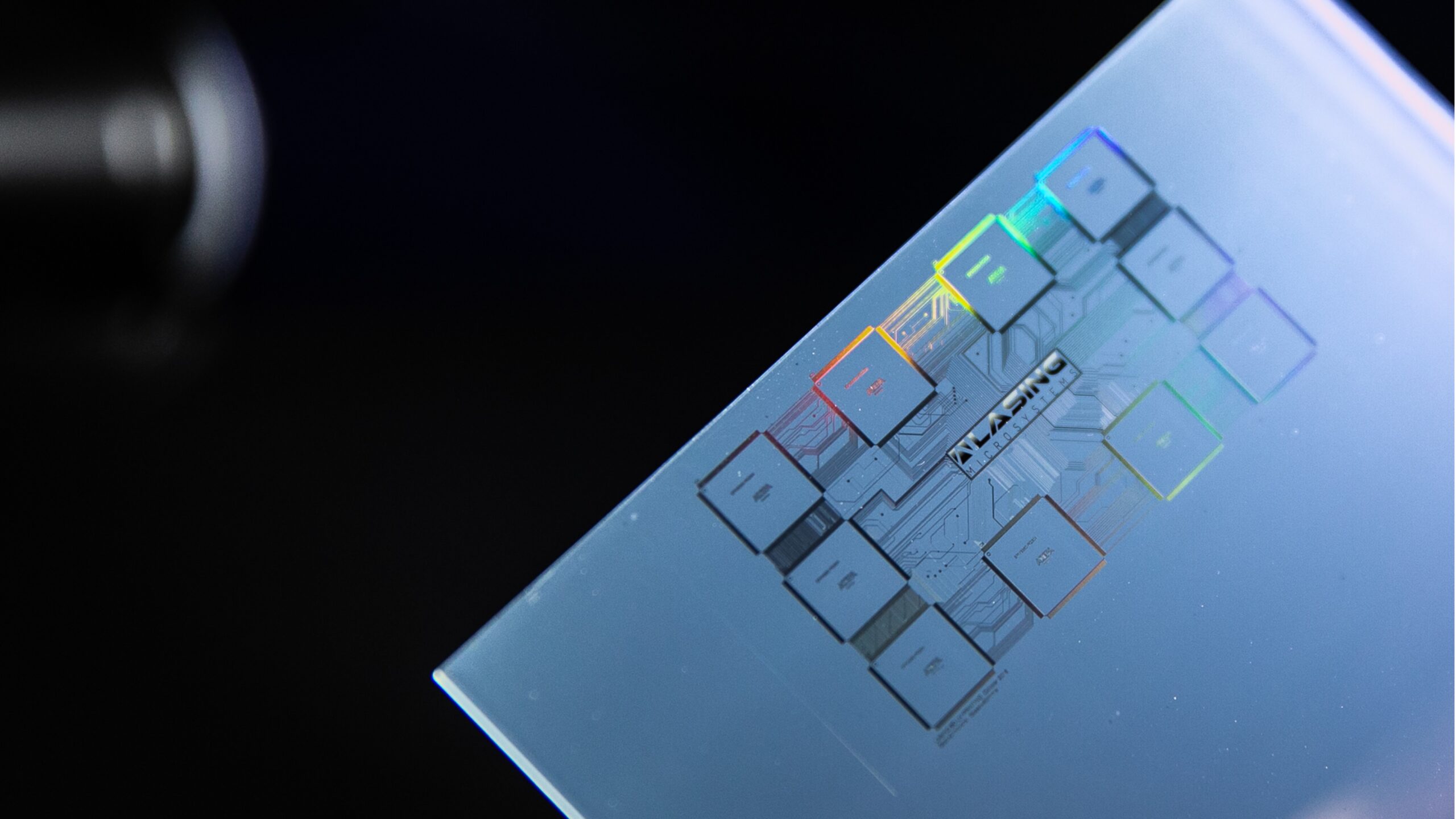
division develops advanced laser material processing systems for multiple applications applied to semiconductors, electronics, medical and precision engineering markets.
· Lasing’s designs integrate the best quality components from leading worldwide companies as Newport and Spectra-Physics, meeting the most demanding requirements.
· Worldwide service, based in distribution support, ensures satisfactory installations with advanced customer trainings and reliable operation.
· Lasing develops advanced programming solutions for each applications market.
Applications
Solar/Photovoltaics Manufacturing
Laser Workstations
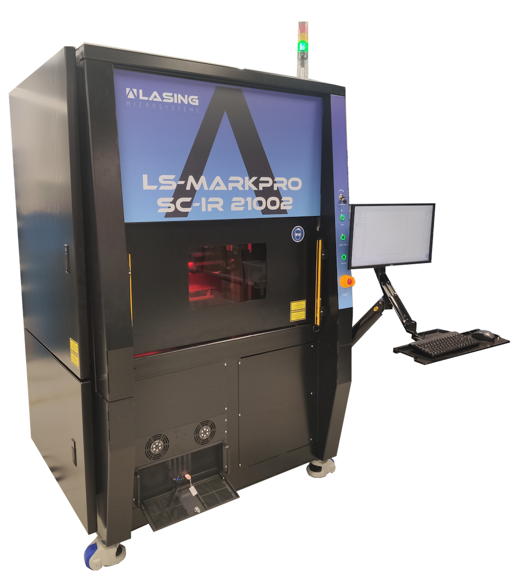
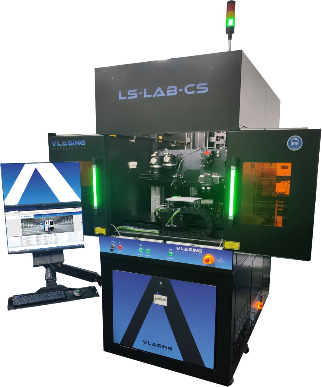
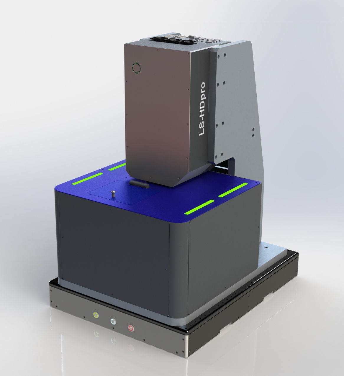
Lasing Microsystems develops versatile and cost effective laser processing machines for high accuracy applications with nanometer resolutions. Depending on application type and the specifications demanded, we offer LS-MARKPRO and LS-LAB model system´s integrating first-class components from leading partners as Newport, Spectra-Physics, NKT… developing easy to use codeless customized software. For complex applications or specific demands we offer complete machine customization (LS-CUSTOM)
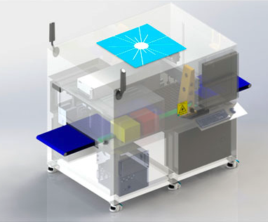
Laser Marking & Engraving
Laser marking is widely used for small, medium and large-scale part marking, identification and traceability in a rapid and flexible process. Patterns include texts, 2D barcodes/data matrices, logos, bitmaps or any geometric shape. The use of cost effective lasers from IR to UV range makes laser marking one of the most demanding application in the market. 3D laser marking Lasing solutions provides with the capability of marking any kind of shape at speeds of m/s.
Laser engraving provides significant advantages in terms of engraving flexibility, depth, surface finishing and “marking” size. High-quality and high speed engraving can be achieved for various materials bare and coated metal, ceramics, glass and polymers and in a broad range of industries as jewelry, fine art/printing modeling, electronics, automotive, and others.

Industrial Manufacturing
Lasers are used for a wide variety of industrial manufacturing applications, including stereolithography, rapid prototyping, laser shock processing, metals and plastic micromachining , intra-glass and other precision marking. The use of the most advanced lasers from Spectra-Physics plus Newport ultra-precise positioning stages let us develop very accurate laser systems with high demand specifications.
Glass Cutting
Spectra-Physics introduces ClearShape™, a patent-pending femtosecond laser process for highest quality, fast cutting of chemically strengthened glass, unstrengthened glass, and sapphire. At speeds over 1000 mm/sec, the new process results in several-fold improvement in cut quality over other laser processes: no chipping, Ra <0.1 µm edge roughness, and as-cut bending strength of >650 MPa for chemically strengthened glass. Using the widely deployed Spirit® family of industrial femtosecond lasers, the new process is ideal for 24/7 manufacturing of displays and windows for mobile devices, wearables, and other demanding applications.
CRFP Cutting
To demonstrate the capability of the Quasar UV laser Spectra-Physics machined 250 µm thick PAN-based CFRP plate material. Parameters varied: pulse width, power, repetition rate, and scanning speed. It is also tested the burst machining capability provided by Quasar’s TimeShift technology.
PCB Drilling
Spectra-Physics is a leading supplier of lasers for the manufacture of printed circuit boards and microelectronics packaging. Spectra-Physics lasers are proven in a wide range of PCB applications including cutting, depaneling, via hole drilling, direct imaging, trimming, repair and marking. With thousands of lasers deployed in demanding PCB applications, Spectra-Physics delivers a broad portfolio of highly reliable, cost-effective lasers backed by our industry-leading global support organization.
Semiconductor and LED Processing
Spectra-Physics is a leading supplier of lasers for the manufacture of semiconductors and LEDs. Spectra-Physics lasers are proven in a wide range of semiconductor and LED applications including LED scribing and lift-off, silicon scribing/dicing, wafer inspection, circuit trimming/repair and many other applications. With thousands of UV lasers deployed in demanding semiconductor and LED applications, Spectra-Physics delivers a broad portfolio of highly reliable, cost-effective lasers backed by our industry-leading global support organization.
Medical Applications
Due to its unique capabilities, laser processing has become the predominant method of cutting, ablating, and welding materials for stent manufacturing. Compared to other cutting methods, laser processing produces very smooth edges that substantially reduce the finishing process. Another laser processing benefit is the ability to make intricate design cuts with extreme precision and accuracy.
Laser Cutting of Stents
In the case of metal stents, including drug-eluting ones, shrinking dimensions allow their deployment in smaller coronary, peripheral and neurovascular blood vessels – important target areas for treatment. Some studies have also suggested a correlation between clinical outcomes and the amount of metal deployed within the vessel. Stent makers have therefore been motivated to work with thinner-walled and smaller-diameter tubes with more complex features.
To demonstrate the capability of femtosecond lasers for the fabrication of these devices, we micromachined ultrafine stent structures in thin-walled nitinol tubes. Out of a 4.25-mm-diameter tube with a wall thickness of 45 µm, a stent-like structure was machined, leaving only 35-µm-wide struts.
Our Partners
